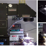
Opto-Electrical Device Characterization Laboratory
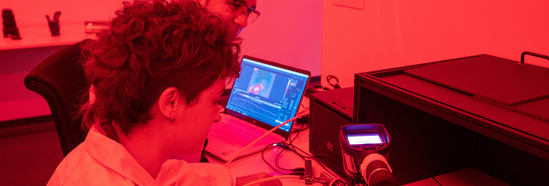
Optoelectronic Device Characterization Laboratory infrastructure is suitable for measuring significant quantities of the device optoelectronic behaviour such as photocurrent, quantum efficiency, spectral response optical response speed and many others.
Lab. Manager:
Services:
- Quantum Efficiency measurement
- J-V measurements
- Impedance analysis
- Spectral and Optical response
Equipment:
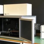
Quantum efficieny
The PVE300 is a turnkey solution for the determination of solar cell spectral response/
EQE (IPCE) and IQE. A range of options include mounts for substrate, superstrate or packaged devices, integrating sphere accessory for measurements of total reflectance and transmittance, a choice of single or multiple channel bias sources, including an AM1.5 matched bias source and a motorised XY stage for device mapping.
Fabrication step: Micro and nano fabrication
Purpose: Characterization of solar cell spectral response/EQE (IPCE) and IQE.
Material systems: Polymers, organics, dielectrics, metals and semiconductors
Node: Materials
Specifications/resolution: The standard spectral range of 300-1100nm, may be extended to 1800 nm and beyond
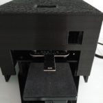
Solar Simulator
A Solar Simulator is a light source that approximates the illumination of natural sunlight. Solar simulators with various tailored spectral output are used to to test a variety of samples including but not limited to solar cells, sun screen (SPF), materials photo-stability, and other samples (in-vivo or in-vitro) under controlled, repeatable, laboratory conditions.
Fabrication step: Micro and nano fabrication
Purpose: J-V curves of solar cell devices as well as long-term stability test under illumination.
Material systems: Polymers, organics, dielectrics, metals and semiconductors
Node: Materials
Specifications/resolution: Factory certified Class AAA CW solar simulator
Newport Oriel-SOL 3A Class AAA (2"x2") 2017
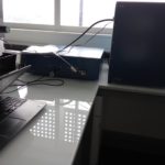
Four points probbing system
The Ossila Four-Point Probe System offers the following benefits for your research:
- Wide range of sheet resistance measurements from 10 mΩ/□ to 10 MΩ/□
- Protect fragile samples from damage with the spring-loaded probes
- Compact size enables use in busy labs with limited space
- Easy-to-use PC software with sheet resistance, resistivity, & conductivity measurements
- Faster material characterisation with automatic correction factor calculation
- Measurements can be repeated easily with saved settings
Fabrication step: Micro and nano fabrication
Purpose: Rapid measurement of sheet resistance, resistivity, and conductivity of materials.
Material systems: Polymers, organics, dielectrics, metals and semiconductors
Node: Materials
Potenciostat
SP-300 is a 500 mA to 10 A state-of-the-art research grade potentiostat/galvanostat/EIS with remarkable specifications such as 7 mHz max frequency, floating mode, analog filtering, built-in calibration board, and stability bandwidths.
The SP-300’s modular chassis accept an optional high current/high voltage option board.
Alternatively, the SP-300 can accept a second potentiostat board (either standard or EIS) and perform as a Bipotentiostat to perform RRDE experiment. It is also a multiple user system as each channel board can be used independently by two different researchers.
Fabrication step: Micro and nano fabrication
Purpose: Electronic characterization of solar cell devices as well as organic material.
Material systems: Polymers, organics, dielectrics, metals and semiconductors
Node: Materials
Specifications/resolution:
- Up to 2 channels
- Compliance: ±12 V up to ±49 V with booster
- Control voltage: ±10 V up to ±48 V with booster
- Potential resolution: 1 µV
- EIS measurement: 10 μHz – 3 MHz (1%, 1°), 10 μHz – 7 MHz (3%, 3°)
- EIS quality indicators
- Current ranges: 1 A to 10 nA (standard)
- Maximum current: ±500 mA (standard)
- Current resolution: 760 fA (standard)
- Low current: 6 ranges from 100 nA to 1 pA with resolution to 76 aA
- Floating mode
- Analog filtering
- Calibration board
- Full stability control mode (9 bandwidths)
Bio Logic Science Instruments-SP-300 2017


 . Afterwards,