Materials Synthesis Laboratory
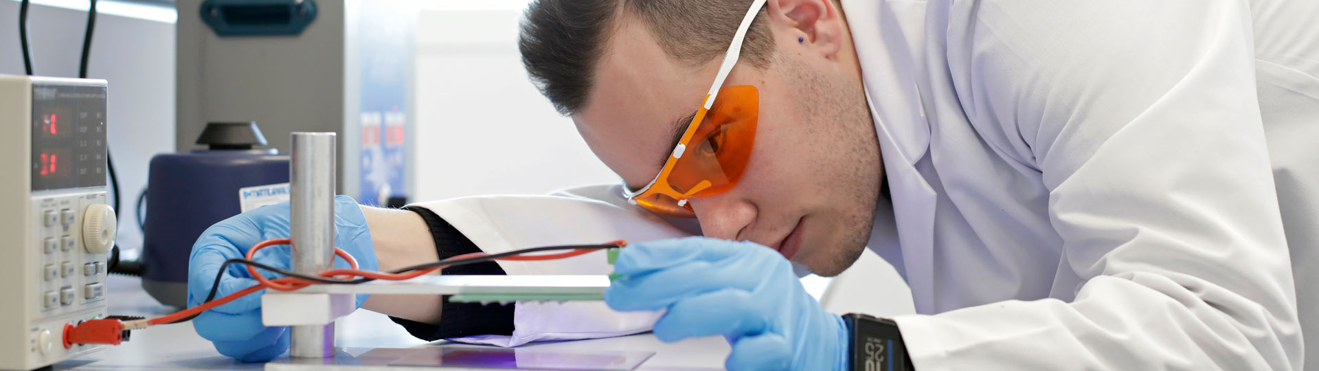
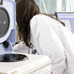
Materials Synthesis Laboratory infrastructure is dedicated to the development and fabrication of perovskite solar cells. In this laboratory it is carried out the major part of the synthesis and assembly of the solar devices.
Also, DSC measurements are possible as well as 2D-printing. This inkjet-printing technology allow as to the fabrication of a wide variety of flexible devices
Lab. Manager:
Services:
- Perovskite solar cell fabrication
- DSC measurements
- 2-D inkjet-printing
- Contact angle measurement
- Deposition of metal contact by thermal evaporation
Equipment:
Contact angle measurement
Contact Angle Goniometer provides a fast, reliable, and easy method to measure the contact angle of a droplet on a surface.
Fabrication step: Micro and nano fabrication
Purpose: Contact-angle measurements and evaluation of hydrophobicity in substrates.
Material systems: Polymers, organics, metals and semiconductors
Node: Materials
Specifications/resolution: High-quality videos of solvent droplets using the high-resolution camera and a specially selected imaging lens.
Difeerential Scanning Calorimetry
Differential Scanning Calorimeter (DSC) with temperature Range from -70 ºC to 730 ºC
Climatic chamber with Temperature range from -40°C to 180°C and Relative Humidity range from 10% to 98% within the temperature range [+5°C; +95°C]
Perkin Elmer-N5360021 (P/N) 2013
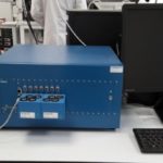
Potenciostat
The VMP3 is a research-grade multi-channel potentiostat. With its modular chassis design, up to 16 independent potentiostat channels can be installed. The VMP3 can be equipped with additional capabilities, including low current measurement, impedance and high current via plug-in modules.
Each potentiostat installed in the VMP3 can be connected to an external high current booster channel, making it ideal for battery studies.
All multichannel potentiostat are multiple user system. Thanks to the Ethernet LAN connection capability, several computers can be connected to the unit at the same time.
Fabrication step: Micro and nano fabrication
Purpose: Electronic characterization of batteries.
Material systems: Batteries.
Node: Materials
Scale/volume: 16 independent potentiostat channels
Specifications/resolution:
- Min current dynamic: +/-100 pA
- Min with LC/ULC option: +/-100 fA
- Max current dynamic: +/-500 mA
- Max with current booster option: +/-150 A
- Voltage range: -10 V to +10 V
- EIS: up to 7 MHz
Bio Logic Science Instruments-VMP3 2012
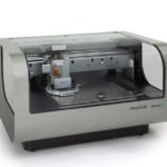
2D Printer
The DMP-2850 allows the deposition of fluidic materials on an 8×11 inch or A4 substrate, utilizing a disposable piezo inkjet cartridge. This printer can create and define patterns over an area of about 200 x 300 mm and handle substrates up to 25 mm thick with an adjustable Z height. The temperature of the vacuum platen, which secures the substrate in place, can be adjusted up to 60°C. The DMP-2850 offers a variety of patterns using a pattern editor program. Additionally, a waveform editor and a drop-watch camera system allows manipulation of the electronic pulses to the piezo jetting device for optimization of the drop characteristics as it is ejected from the nozzle. This system enables easy printing of structures and samples for process verification and prototype creation.
MEMS-based cartridge-style print-head that allows users to fill their own fluids and print immediately with the DMP in their own laboratory. To minimize waste of expensive fluids, each cartridge reservoir has a capacity of 1.5 ml. Cartridges can easily be replaced to facilitate printing of a series of fluids. Each single-use cartridge has 16 nozzles linearly spaced at 254 microns with typical drop sizes of 1 and 10 picoliters.
Fujifilm Dimatix-DMP-2850 2017
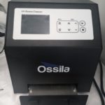
UV Ozone Cleaner
Ossila’s UV Ozone cleaning system is capable of removing contamination on the surface of samples, providing you with ultraclean surfaces within minutes. By using a high-power UV light source, ozone is generated – which then breaks down surface contaminants into volatile compounds. These volatile compounds evaporate from the surface leaving no trace. This method can produce near-atomically clean surfaces without causing damage to the sample.
Fabrication step: Micro and nano fabrication
Purpose: Cleaning and modified substrates surfaces in the manufacture of organic electronics and semiconductors for application areas such as polymer photovoltaics.
Material systems: Glass, FTO substrates
Node: Materials
Specifications/resolution: UV ozone cleaner houses a 120mm x 120mm tray for positioning samples under the UV light source.
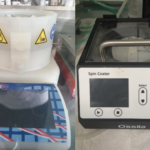
Spin coater
Spin-coating is used to apply uniform thin films to flat substrates. The film material is dissolved in a moderate boiling point material and applied to a substrate that is undergoing rotation, typically 500-2000 rpm. The thickness of film is determined by the concentration of the solution or dispersion and the rotation speed and spin time.
This particular spin coater is used to apply thin (100 nm) films to FTO-coated glass for the fabrication of organic electronic devices.
Fabrication step: Micro and Nano Fabrication
Purpose: Deposition of thin polymer/organic films from solution or dispersion
Material systems: Polymers, organics, dielectrics, metals, semiconductors, glasses and ceramics
Node: Materials
Scale/volume: Up to 4 inch substrates
Specifications/resolution: Polypropylen
Heat treatment
High-performance hotplate for temperatures up to 600°C with a very short heating-up time (600°C within 20 minutes). The extremely efficient insulation allows the appliance to also be used on working surfaces which are not heat-resistant. The insulated hinged lid has been designed to keep heat loss to the absolute minimum.
The temperature can either be controlled with a temperature or programme controller. With the temperature controller the hotplate’s complete heating surface is held at a constant selected temperature.
In addition, ovens are microprocessor controlled, with an LED display of time and temperature. Samples can be dried, under a temperature accuracy from 5°C above room temperature to 300°C, and providing remarkably short heating and recovery times as well as reproducible results.
Fabrication step: Micro and nano fabrication, Chemical synthesis
Purpose: Thermal treatment of organic electronics and semiconductors for application areas such as polymer photovoltaics, OLEDs or transistors and the purification steps un organic synthesis.
Material systems: Polymers, organics, dielectrics, metals and semiconductors
Node: Materials
Scale/volume: 600°C (Hot-plates) and 300°C (Ovens)
Multiple
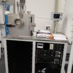
Thermal evaporator
The thermal evaporator is a multi-source metal deposition system which allows metal coatings to be deposited either sequentially or by co-deposition, at a controlled thickness through a mask. The multi-source evaporator is built into a four port glove box, allowing sample handling under inert conditions and also incorporates a spin-coater. Passivating metal or metal oxide layers can be deposited, and complete devices can be assembled in non-oxidative conditions.
This facility enables the fabrication of a wide range of micro and nano-scale devices; target specific electrodes after further modification in a range of sensors; top electrodes in organic photovoltaic devices, contacts in organic diodes and transistors.
Fabrication step: Micro and nano fabrication
Purpose: Deposition of thin films by thermal evaporation and spin coating under vacuum
Material systems: Any
Node: Materials
Scale/volume: 4 inch diameter wafers
Specifications/resolution: Angstrom film thickness resolution
Moorfield Minilab-LT60A 2017
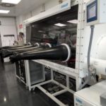
Glove Box
A glove box provides a working space that is isolated from the outside (room) atmosphere. It maintains an atmosphere of pure nitrogen in which the concentration of oxygen and moisture is typically below 1 ppm.
Products sensitive to oxygen and/or water vapour can be handled in this atmosphere through the gloves. This glove box contains equipment used to characterise organic solar cells.
Fabrication step: Micro and nano fabrication
Purpose: Manufacture of organic electronics and semiconductors for application areas such as polymer photovoltaics, OLEDs or transistors and related organic electronic components.
Material systems: Polymers, organics, dielectrics, metals and semiconductors
Node: Materials
Scale/volume: 4 glove boxes
Specifications/resolution: Argon atmosphere. Integrated spin coating and thin film deposition systems.
MBraun-Unilab Pro Eco SP 2018


 . Afterwards,